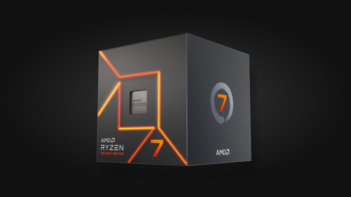
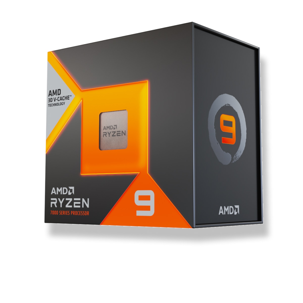
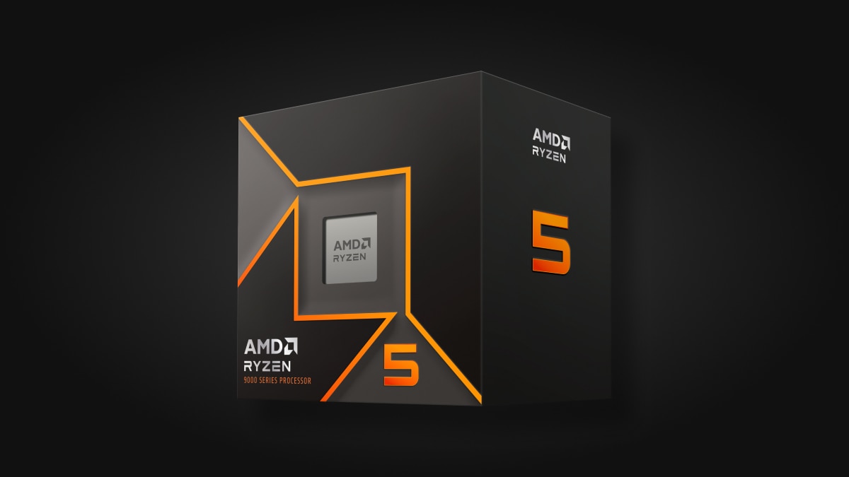
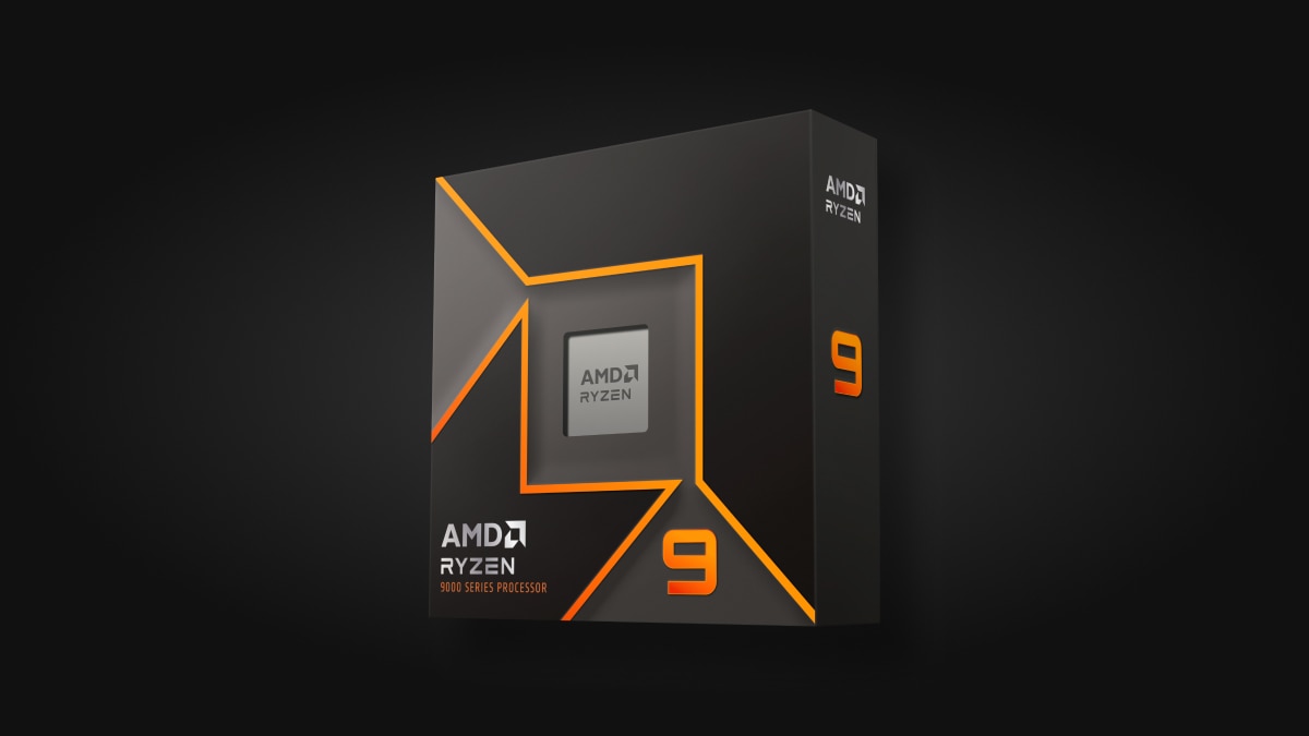
AMD Ryzen 9 9900X
A 12-core, 24-thread Zen 5 desktop processor for socket AM5 with a 120 W default TDP, up to 5.6 GHz boost, 64 MB of L3 cache, DDR5 and PCIe 5.0, sold without a cooler.
Full Specification Sheet
| Architecture | Zen 5 (codename Granite Ridge) |
|---|---|
| Cores / Threads | 12 / 24 |
| Base Clock | 4.4 GHz |
| Max Boost Clock | Up to 5.6 GHz |
| L1 Cache | 960 KB |
| L2 Cache | 12 MB |
| L3 Cache | 64 MB |
| Default TDP | 120 W |
| Process | TSMC 4nm FinFET (CPU cores), TSMC 6nm FinFET (I/O die) |
| Package Die Count | 3 |
| Socket | AM5 |
| Memory | DDR5, 2 channels, up to 256 GB, DDR5-5600 (2 x 1R or 2 x 2R), DDR5-3600 with four modules |
| PCIe | PCIe 5.0, 28 lanes (24 usable) |
| USB | 4 x native USB 3.2 Gen 2 (10 Gbps), 1 x USB 2.0 |
| Integrated Graphics | AMD Radeon Graphics, 2 cores, 2200 MHz |
| Unlocked | Yes (Precision Boost Overdrive, Curve Optimizer, AMD EXPO) |
| Max Operating Temperature | 95 C |
| Cooler Included | No (liquid cooler recommended by AMD) |
| Product ID | 100-100000662WOF (boxed), 100-000000662 (tray) |
The AMD Ryzen 9 9900X is a twelve-core desktop processor from the Ryzen 9000 Series, built on the Zen 5 architecture under the former codename Granite Ridge. AMD describes it as an incredibly powerful processor for gaming and streaming, and the specification supports that framing: twelve cores and twenty-four threads, a boost clock of up to 5.6 GHz and a default thermal design power of 120 W, all on the AM5 socket. The manufacturer page gives a launch date of 15 August 2024 and no price, so this entry records the date and leaves the price empty. Everything below comes from AMD's published specification table, with a few clearly labelled calculations. We have not benchmarked the chip ourselves, and we do not repeat the vendor's own gaming claims.
Cores, clocks and cache
AMD lists 12 CPU cores with simultaneous multithreading, which gives 24 threads. The maximum boost clock is up to 5.6 GHz and the base clock is 4.4 GHz. AMD explains the two terms in its footnotes: maximum boost is the highest frequency a single core can reach on a bursty single-threaded workload and varies with the thermal paste, the cooling, the motherboard design, the BIOS, the chipset driver and the operating-system updates, while the base clock is the average effective base frequency of all cores. The cache hierarchy is 960 KB of L1, 12 MB of L2 and 64 MB of L3. The L2 figure works out to 1 MB per core, and the L3 figure to about 5.3 MB per core (64 divided by 12). Our explainer on core count versus clock speed shows why a chip like this can make sense for people who mix gaming with rendering, compiling or streaming: the extra cores matter when several heavy tasks run at once, while the high boost clock matters for the lightly threaded work that most games still lean on.
Process technology and packaging
The CPU cores use TSMC 4nm FinFET technology and the I/O die uses TSMC 6nm FinFET. The page lists a package die count of three, which is consistent with the multi-die design AMD uses across the Ryzen 9 family: compute dies plus a separate I/O die. The page does not say how the twelve cores are divided between compute dies, and it does not publish die sizes for this model, so we do not guess at the split. What it does confirm is that the processor is unlocked for overclocking. AMD adds a warranty footnote here: the product warranty does not cover damage caused by overclocking, even when overclocking is enabled through AMD hardware or software. The supported tuning features are AMD EXPO memory overclocking technology, Precision Boost Overdrive, Curve Optimizer voltage offsets and Ryzen Master support.
Power and cooling
The default TDP is 120 W and the maximum operating temperature (Tjmax) is 95 C. The page states that no thermal solution is included and that a liquid cooler is recommended for optimal performance. That is a real cost to plan for: the processor ships without any cooler, so a cooler has to be bought separately and has to fit the AM5 mounting pattern. Our comparison of air and liquid cooling covers the trade-offs, including noise, clearance and maintenance. A recommendation is not a requirement, and a good air cooler can hold a 120 W part, but the manufacturer's wording tells you how it expects the chip to be used when it boosts hard.
Memory and platform
The processor uses socket AM5 and supports DDR5 only, in two channels, with unbuffered DIMMs and up to 256 GB. The page lists the maximum memory speed as DDR5-5600 for two single-rank modules and for two dual-rank modules, and DDR5-3600 for four modules of either rank type, which is a useful reminder that filling all four slots lowers the guaranteed speed. As arithmetic, two channels of DDR5-5600 move 5600 million transfers per second times 8 bytes times two channels, or 89.6 GB/s of peak theoretical bandwidth. ECC is listed as supported when the motherboard supports it. Supporting chipsets are A620, B650, B650E, X670, X670E, B840, B850, X870 and X870E, so the processor fits both older and newer AM5 boards after the usual BIOS check. For the wider picture of sockets and generations, our AM4, AM5 and LGA1700 platform guide is a good companion.
Connectivity and graphics
The processor offers PCIe 5.0 with 28 native lanes, of which 24 are usable. The page then lists additional usable lanes that depend on the motherboard chipset: four PCIe 4.0 lanes on X870, eight on X870E, twelve on X670 and X670E, and eight on B650 and B650E. Native USB is four ports of USB 3.2 Gen 2 at 10 Gbps and one USB 2.0 port, and NVMe boot is supported with RAID 0, 1, 5 and 10 modes. The chip also has a small integrated GPU: AMD Radeon Graphics with two graphics cores at 2200 MHz, with USB Type-C DisplayPort Alternate Mode support. Two graphics cores are enough to put an image on a screen for setup, troubleshooting or office work, but they are not a replacement for a discrete graphics card in games. Supported operating systems are Windows 11 and Windows 10 in 64-bit editions, Red Hat Enterprise Linux and Ubuntu in 64-bit builds.
Instruction set and identifiers
The instruction set is x86-64 with the extensions AES, AMD-V, AVX, AVX2, AVX512, FMA3, MMX-plus, SHA, SSE, SSE2, SSE3, SSE4.1, SSE4.2, SSE4A and SSSE3. The boost technology is listed as Precision Boost 2. The boxed product ID is 100-100000662WOF and the tray product ID is 100-000000662, which is what you would quote when checking that a listing matches this exact model rather than the neighbouring X3D or non-X variants.
Where it sits in our database
The nearest relatives in our database are the Ryzen 9 9950X, which lists 16 cores and 32 threads, a 170 W default TDP and a boost clock of up to 5.7 GHz, and the Ryzen 9 9900X3D, which lists the same 12 cores, a 120 W TDP, a 4.4 GHz base clock and 128 MB of L3 cache with second-generation 3D V-Cache, but a slightly lower boost of up to 5.5 GHz. Set against those two, the 9900X is the plain version: the same core count and the same 120 W as the 3D V-Cache model, with half the L3 cache and a 100 MHz higher boost ceiling, and four fewer cores and 50 W less TDP than the 9950X. In cores per watt, 120 W for twelve cores is 10 W per core against about 10.6 W per core for the 9950X, which is arithmetic from the two pages and not a measured efficiency figure. You can read the closest pair side by side in our comparison of the 9900X and the 9900X3D, and the whole processor category is open for wider browsing.
What the page does not say
AMD's page does not list a price, a die-size figure for this model, a split of the cores between dies or any benchmark data we could cite as independent. It also repeats the generic notes about boost behaviour and warranty. If you are choosing between the 9900X and its neighbours, use this entry to check the facts that decide compatibility and cost of ownership: socket and chipset support, memory limits, the absence of a cooler in the box, the 120 W default TDP and the PCIe lane budget. Then look for independent testing that matches the games and applications you actually run before you decide how much cache and how many cores you are willing to pay for.