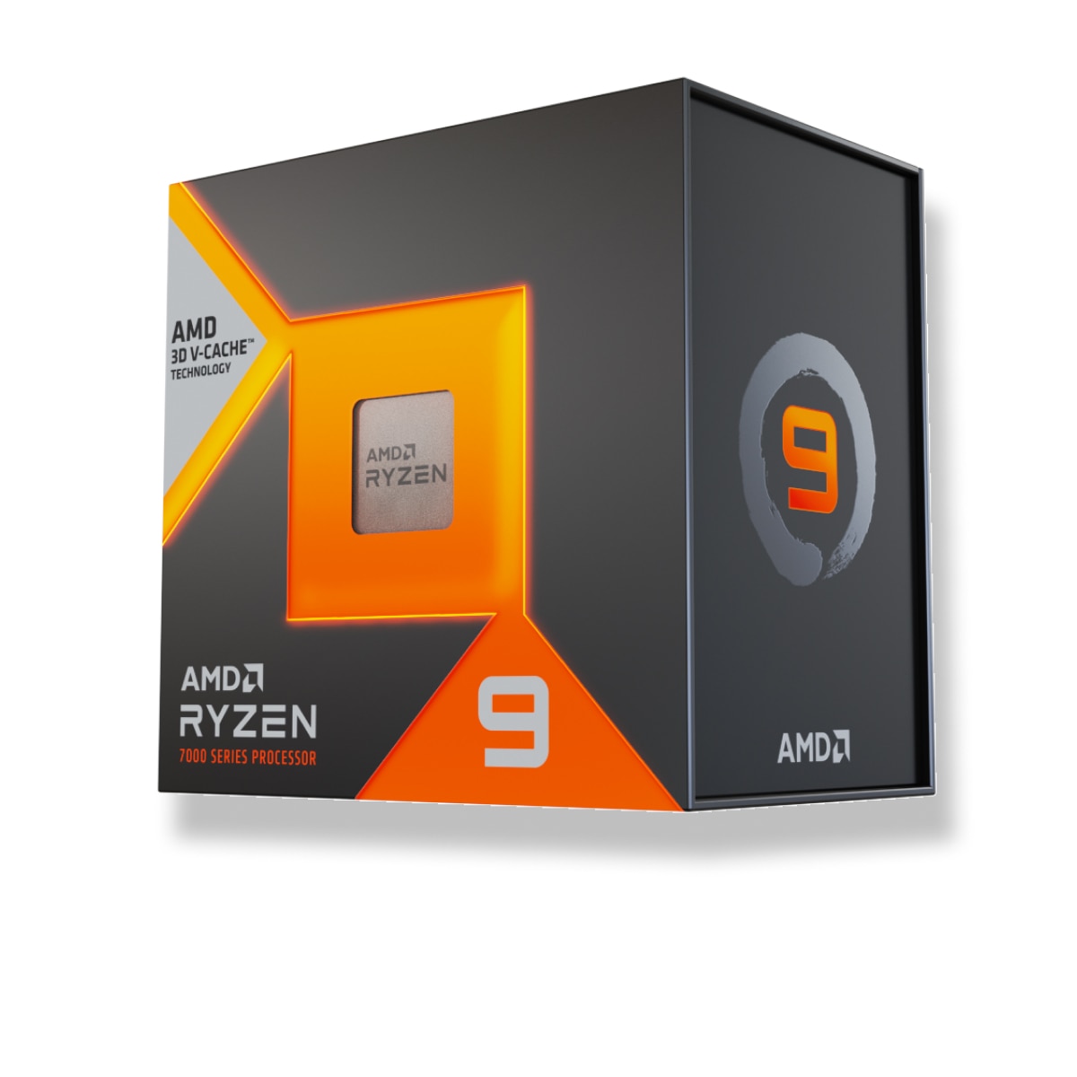
AMD Ryzen 9 7950X3D
A 16-core, 32-thread Zen 4 AM5 processor with AMD 3D V-Cache, 128 MB of L3 cache, a 4.2 GHz base clock, up to 5.7 GHz boost and a 120 W default TDP, launched on 28 February 2023.
Full Specification Sheet
| Architecture | Zen 4 (codename Raphael) |
|---|---|
| Cores / Threads | 16 / 32 |
| Base Clock | 4.2 GHz |
| Max Boost Clock | Up to 5.7 GHz |
| L1 Cache | 1024 KB |
| L2 Cache | 16 MB |
| L3 Cache | 128 MB (AMD 3D V-Cache) |
| Default TDP | 120 W |
| Process | TSMC 5nm FinFET (CPU cores), TSMC 6nm FinFET (I/O die) |
| Socket | AM5 |
| Memory | DDR5, 2 channels, up to 128 GB, DDR5-5200 (2 x 1R / 2 x 2R), DDR5-3600 (4 modules) |
| PCIe | PCIe 5.0, 28 lanes (24 usable) |
| Integrated Graphics | AMD Radeon Graphics, 2 cores, 2200 MHz |
| Unlocked | Precision Boost Overdrive, Curve Optimizer and Ryzen Master supported |
| Cooler Included | No (liquid cooler recommended by AMD) |
| Max Operating Temperature | 89 C |
The AMD Ryzen 9 7950X3D is a sixteen-core desktop processor for the AM5 socket that combines the Zen 4 core design with AMD 3D V-Cache technology. AMD's product page calls it the ultimate processor for gaming and describes it as a 16-core part that can do it all, aimed at the most demanding gamers and creators. It belongs to the Ryzen 7000 Series, carries the former codename Raphael, is sold as a boxed processor in the enthusiast desktop segment and has a launch date of 28 February 2023 on AMD's page. This entry walks through everything the manufacturer publishes, explains what the numbers mean when you are choosing parts, and says plainly where the page stays silent. It contains no benchmarks of our own. AMD's page lists no price, so none is given here, and every figure below is a manufacturer specification unless it is marked as simple arithmetic.
Cores, threads and clocks
AMD lists sixteen CPU cores with simultaneous multithreading, which the operating system presents as thirty-two threads. The base clock is 4.2 GHz, described by AMD as the average effective base frequency of all cores, and the maximum boost clock is up to 5.7 GHz. As on every AMD page, the boost figure is explained as the highest frequency a single core can reach on a bursty single-threaded workload, and it varies with thermal paste, system cooling, motherboard design and BIOS, the chipset driver and operating-system updates. The distance between base and boost is 1.5 GHz (arithmetic from AMD's two figures). For context, the standard Ryzen 9 7950X in our database has the same sixteen cores and the same 5.7 GHz boost, but a 4.5 GHz base clock and a 170 W TDP, so the 3D V-Cache model trades 0.3 GHz of base clock and 50 W of default power budget for a much larger cache. If you want to understand why core count and clock speed pull in different directions, our guide on core count versus clock speed covers the principle without model-specific claims.
Cache: the reason this chip exists
The cache figures are the heart of this model. AMD lists 1024 KB of L1 cache, 16 MB of L2 cache and 128 MB of L3 cache. Dividing the totals across sixteen cores gives 64 KB of L1 and 1 MB of L2 per core, and 8 MB of L3 per core on average (arithmetic from AMD's totals; the page does not say how the L3 is distributed between the compute dies, so we do not describe the split). The plain Ryzen 9 7950X in our database lists 64 MB of L3, so the X3D version doubles the last-level cache. Next to the eight-core Ryzen 7 7800X3D, which lists 96 MB of L3, the 7950X3D carries a third more total L3 and twice as many cores. AMD's marketing line is that the stacked cache gives low latency and extra game performance; the page backs that with a game-testing footnote that we deliberately do not reproduce, because it is vendor test data from December 2022 on one reference setup. Our own explainer on how AMD 3D V-Cache processors work is the right place to read about why large caches help some workloads and barely move others.
Process, packaging and power
The CPU cores use a TSMC 5nm FinFET process and the I/O die uses TSMC 6nm FinFET. AMD gives the size of the CPU compute die as 71 mm squared and the I/O die as 122 mm squared, and lists a package die count of three. The default TDP is 120 W. AMD's page says the thermal solution is not included and recommends a liquid cooler for optimal performance, which is worth taking literally: no cooler comes in the box, so budget for one. The maximum operating temperature (Tjmax) is 89 degrees Celsius, which is lower than the 95 degrees AMD lists for some newer Zen 5 chips, a known trait of the stacked-cache parts. If you plan to push the chip, remember that the page confirms Precision Boost Overdrive, Curve Optimizer voltage offsets and Ryzen Master support, but it does not publish voltage limits, so read our notes on CPU overclocking and voltage safety before changing anything.
Platform: socket, chipsets and memory
The socket is AM5. AMD lists these supporting chipsets: A620, X670E, X670, B650E, B650, X870E, X870, B840 and B850. Memory is DDR5 only, in two channels, with up to 128 GB supported. The listed memory speeds depend on the loading: DDR5-5200 with two single-rank modules, DDR5-5200 with two dual-rank modules, and DDR5-3600 with four modules of either rank type. ECC support is listed as yes, but it requires motherboard support. AMD EXPO memory overclocking is supported. Note the maximum of 128 GB: some newer Ryzen 9000 pages list 256 GB, so if you plan a very large capacity build the generation matters. The PCI Express version is 5.0 with 28 native lanes, 24 of them usable. AMD adds usable lanes from the motherboard depending on the chipset, for example 12 Gen4 lanes on X670E and X670 and 8 Gen4 lanes on B650E and B650. Native connectivity is four USB 3.2 Gen 2 (10 Gbps) ports, no USB 3.2 Gen 1 ports, one USB 2.0 port and no native SATA ports, so SATA storage always comes from the chipset. NVMe boot is supported, with RAID 0, RAID 1 and RAID 10 listed. To see how these chipset tiers differ in practice, read our motherboard chipset tiers explained page.
Integrated graphics and extras
Unlike the F-suffix chips of other families, this processor includes basic graphics: AMD Radeon Graphics with two graphics cores at 2200 MHz, and USB Type-C DisplayPort Alternate Mode is listed as supported. Two graphics cores are enough to put an image on a screen for setup, troubleshooting or office use, but they are not a gaming solution. The instruction set is x86-64 with AES, AMD-V, AVX, AVX2, AVX512, FMA3, SHA, the SSE family and others. AMD lists support for Windows 11 and Windows 10 in 64-bit editions, Red Hat Enterprise Linux and Ubuntu. The boxed product ID is 100-100000908WOF and the tray ID is 100-000000908.
Where it sits in our database
Within the CPU category the 7950X3D is a bridge between two worlds: it has the core count of the 7950X for heavy multithreaded work and the large cache of the 7800X3D for games that like cache. Our database also holds the newer Zen 5 Ryzen 9 9950X3D, which lists 16 cores, 128 MB of L3, a 4.3 GHz base clock and a 170 W TDP on a 4nm process with 256 GB memory support. If you are deciding between the two generations, the side-by-side comparison of the 7950X3D and the 9950X3D puts every listed figure next to the other, and the full processor category lets you widen the search.
What the page does not say
AMD's page does not state a price, does not say how the cache is divided between dies, does not publish PBO limits or voltage ceilings, and does not list a retail cooler recommendation beyond the general liquid-cooler line. It also includes a performance chart footnote based on AMD's own testing; we treat it as marketing context and do not repeat figures from it. Treat the entry here as a compact, accurate summary of the manufacturer's specification, and verify details such as BIOS requirements for your exact motherboard with the board maker before you buy.